
A tour of the interface
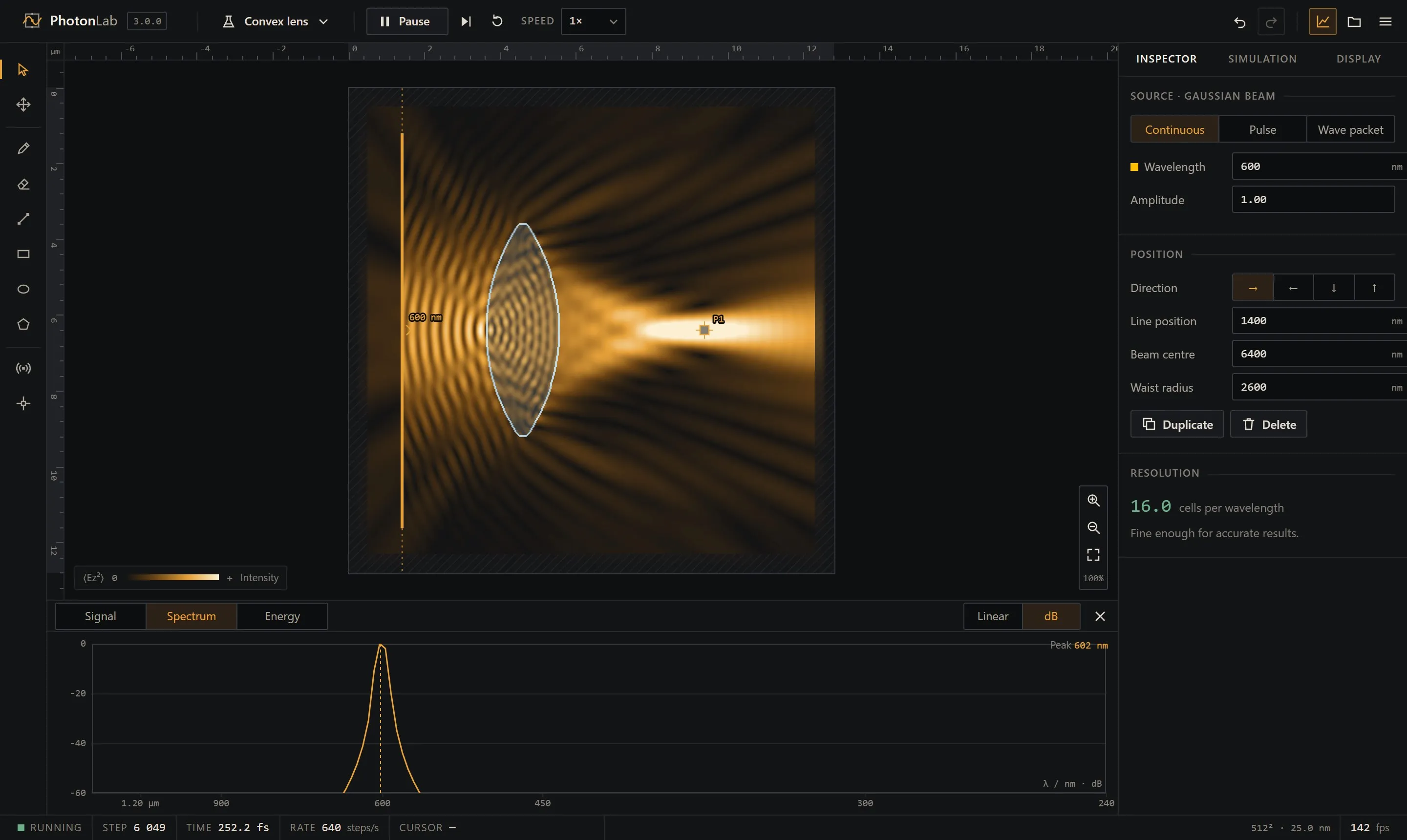
The layout follows a bench instrument: controls along the edges, the measurement in the middle, readouts at the bottom.
Top bar
Section titled “Top bar”From left to right:
- PhotonLab and the version. Click it for the about box, which also shows the grid size and whether the renderer runs in the worker.
- Experiments (flask icon). The built-in scenes, grouped by topic, and New empty scene.
- Run / Pause, Step and Reset. Reset clears the fields and restarts the clock but keeps your geometry, sources and probes.
- Speed. At 1× light crosses the domain in about 1.6 seconds, whatever the grid size. If your device cannot keep up, the status bar says so.
- Undo / Redo, the analysis panel toggle, the file menu (open, save, share, PNG, video, CSV) and the menu with language, shortcuts and documentation.
Tool rail
Section titled “Tool rail”The column on the left holds the tools: select, pan, brush, eraser, line, rectangle, ellipse, polygon, source and probe. Each has a single-key shortcut, shown when you hover over it. See Drawing and materials.
The view
Section titled “The view”The square is the simulation domain. The rulers are in micrometres. The hatched band around the edge is the absorbing layer; fields inside it are not physical, so do not place probes there.
Materials are drawn on top of the field: dielectrics as a tint with an outline, metals with diagonal hatching, the absorber with cross hatching.
Scroll or pinch to zoom, and drag empty space with the select tool to pan. F fits the domain to the window again.
The legend in the lower left shows which quantity and colour map you are looking at. In the default Phosphor map, amber is positive field, blue is negative and black is zero.
Inspector
Section titled “Inspector”The panel on the right has three tabs.
- Inspector changes with what you are doing. With a drawing tool active it shows the material palette and brush width. With a source or probe selected it shows that object’s settings. At the bottom it always shows the resolution: how many grid cells cover one wavelength in the densest material on screen. Green means the result can be trusted; amber or red means the grid is too coarse for that material and wavelength (see Units and resolution).
- Simulation: polarization (TM or TE), boundary type for each pair of edges, the physical size of the domain and the grid size.
- Display: field or time-averaged intensity, exposure, colour map, and whether to draw materials and the absorbing layer.
On tablets the inspector slides over the view; toggle it with I. On phones it is a sheet that slides up from the bottom.
Analysis panel
Section titled “Analysis panel”Press A. It has three tabs: the probe signal over time, its spectrum, and the total energy in the domain. See Probes and spectra.
Status bar
Section titled “Status bar”The strip at the bottom is the instrument readout: running state, time step, simulated time in femtoseconds, how many steps per second the device achieves, the cursor position with the material under it, the grid size with the physical cell size, and frames per second.
On a phone
Section titled “On a phone”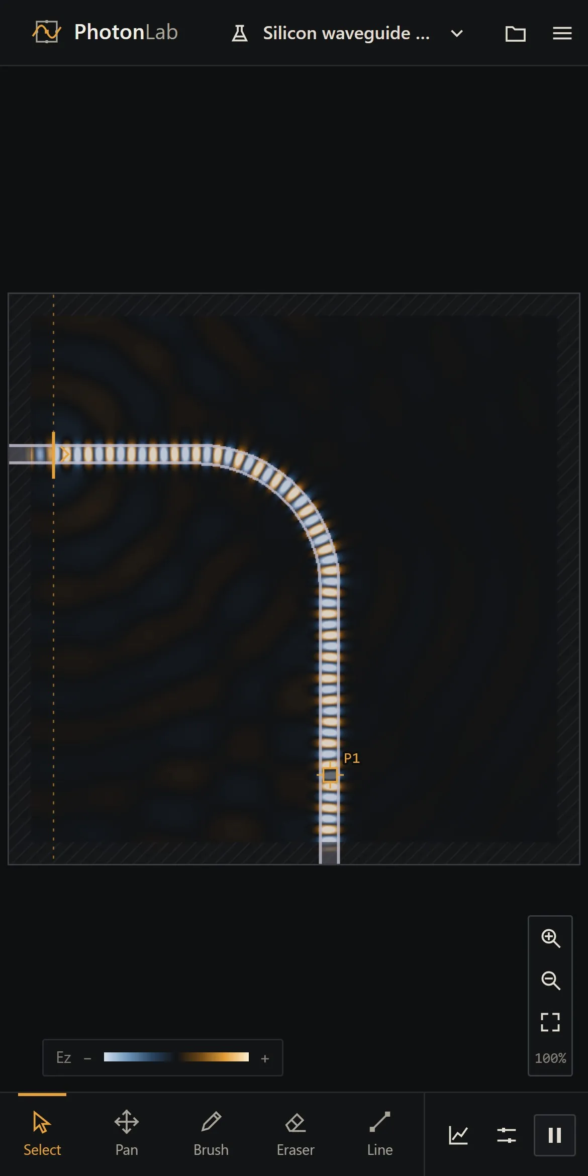
The tools move to a bar at the bottom. Two fingers always pan and zoom, one finger uses the current tool. The run button, the analysis panel and the inspector sit at the right end of the bar. Step, reset, undo and speed are in the top-right menu.